

File:Amstrad PCW8256 monitor PCB layout.png
Size of this preview: 436 × 599 pixels. Other resolution: 1,602 × 2,200 pixels.

Original file (1,602 × 2,200 pixels, file size: 1.93 MB, MIME type: image/png)
Summary
[edit | edit source]

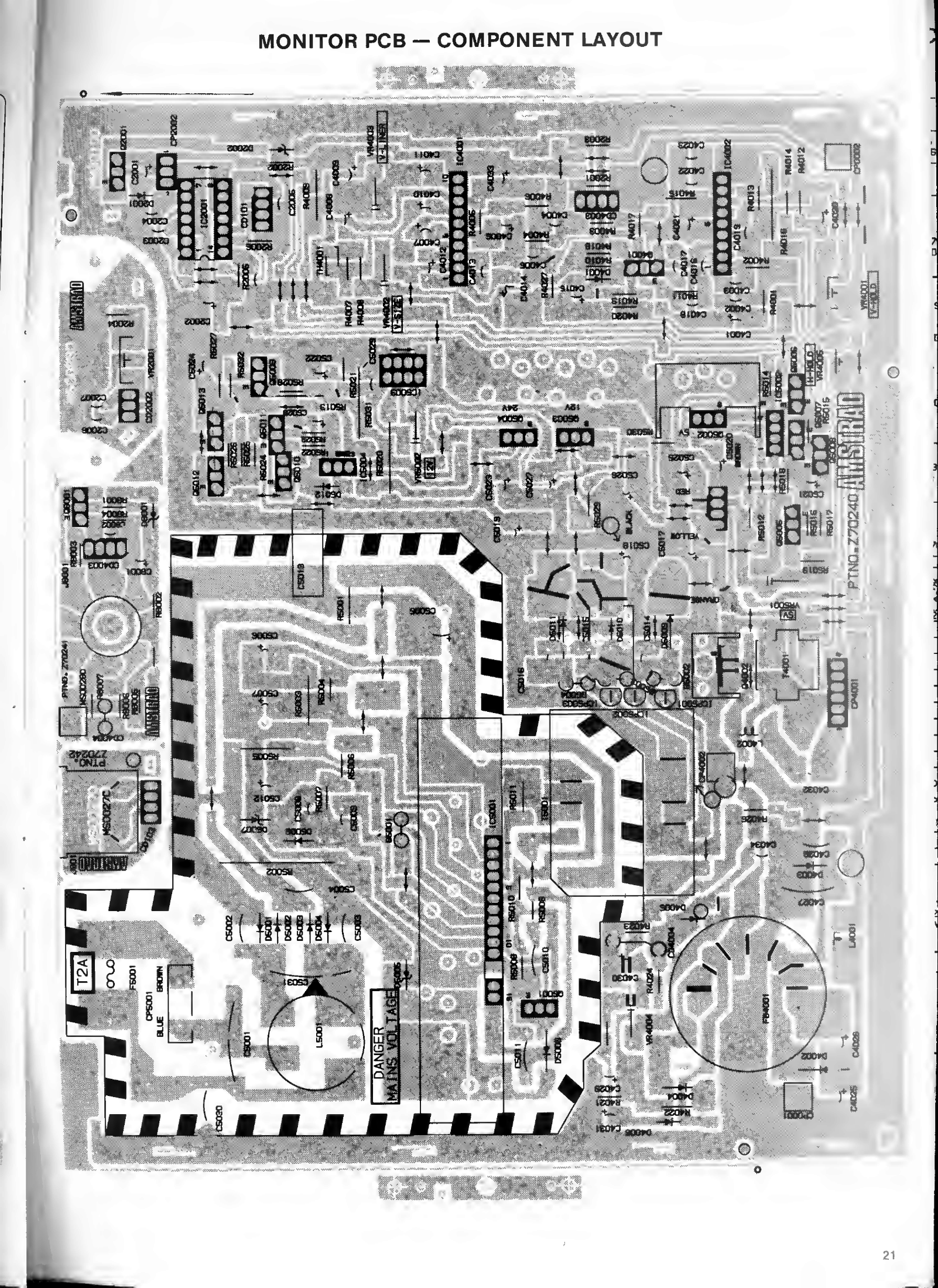
Component layout of the PCW8256/8512 monitor board, which carries the switch-mode power supply, the deflection circuits and the mains input with fuse F5001 (marked T2A). The hatched outline marks the area at mains potential ("danger mains voltage").
Source
[edit | edit source]

Rendered at 400 dpi from the hosted File:Amstrad PCW 8000 Series Service Manual.pdf (Amstrad, PCW 8256/8512 Personal Computer Word Processor Service Manual), PDF page 22, with the contrast increased.
Author
[edit | edit source]

Amstrad plc.
Licence
[edit | edit source]

Copyright Amstrad plc. Hosted for preservation and repair reference, with the source cited.
File history
Click on a date/time to view the file as it appeared at that time.
| Date/Time | Thumbnail | Dimensions | User | Comment | |
|---|---|---|---|---|---|
| current | 06:20, 2 October 2026 | | 1,602 × 2,200 (1.93 MB) | Josh (talk | contribs) | Upload for the Amstrad PCW/PPC pages |
You cannot overwrite this file.
File usage
The following 3 pages use this file:
