

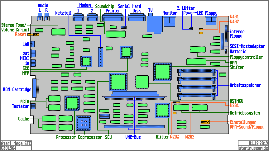
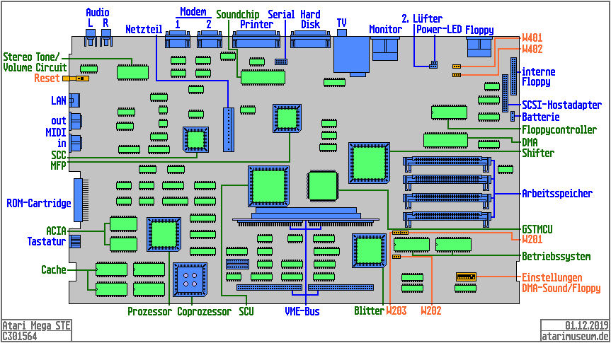
File:Atari Mega STE board layout C301564.png

Summary
[edit | edit source]

Layout drawing of the Atari Mega STE main board, PCB C301564, labelled in German: ports along the top edge, LAN, MIDI, ROM cartridge, keyboard connector, cache, CPU and coprocessor sockets, SCU, VME bus header, Blitter, the ROM jumpers W201–W203, TOS ROMs, SIMM sockets (Arbeitsspeicher), GSTMCU, Shifter, DMA, floppy controller, battery connector, SCSI host-adapter header, internal floppy, power LED and second-fan headers, jumpers W401/W402 and the DMA-sound/floppy DIP switch. Drawn 1 December 2019.
Source
[edit | edit source]

https://www.atari-computermuseum.de/bilder/st/mb_mste.gif (converted to PNG), from the page https://www.atari-computermuseum.de/megaste.htm (retrieved 2026-10-01)
Author
[edit | edit source]

atari-computermuseum.de
Licence
[edit | edit source]

Copyright atari-computermuseum.de (Atari Museum Deutschland); no licence stated. Used to identify the product. Reproduced as a component location map.
File history
Click on a date/time to view the file as it appeared at that time.
| Date/Time | Thumbnail | Dimensions | User | Comment | |
|---|---|---|---|---|---|
| current | 00:19, 1 October 2026 | | 863 × 485 (19 KB) | Josh (talk | contribs) | Mega STE board layout drawing (atari-computermuseum.de) |
You cannot overwrite this file.
File usage
The following 3 pages use this file:
