

File:Sega Dreamcast VA0 block diagram.png

Summary
[edit | edit source]

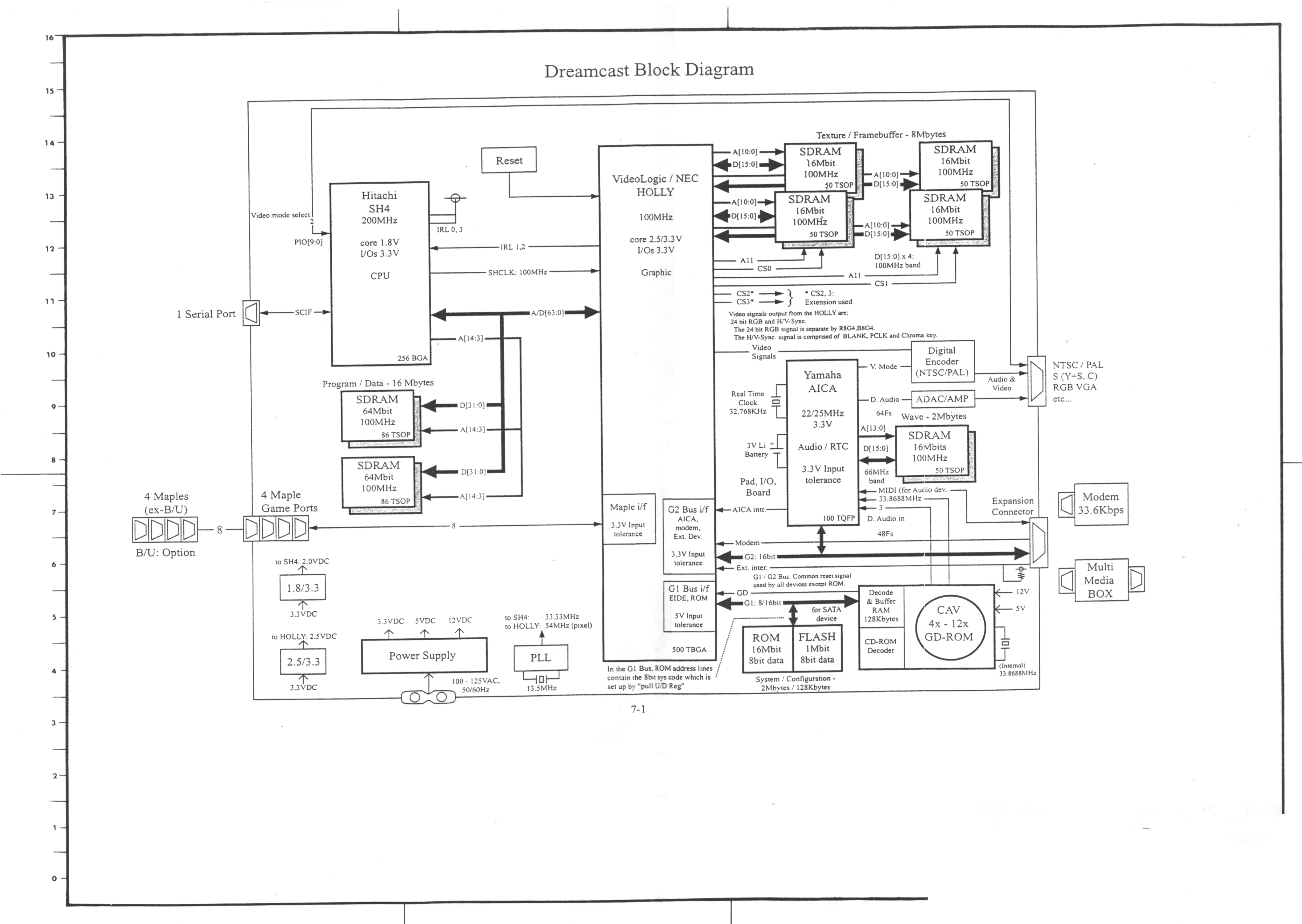
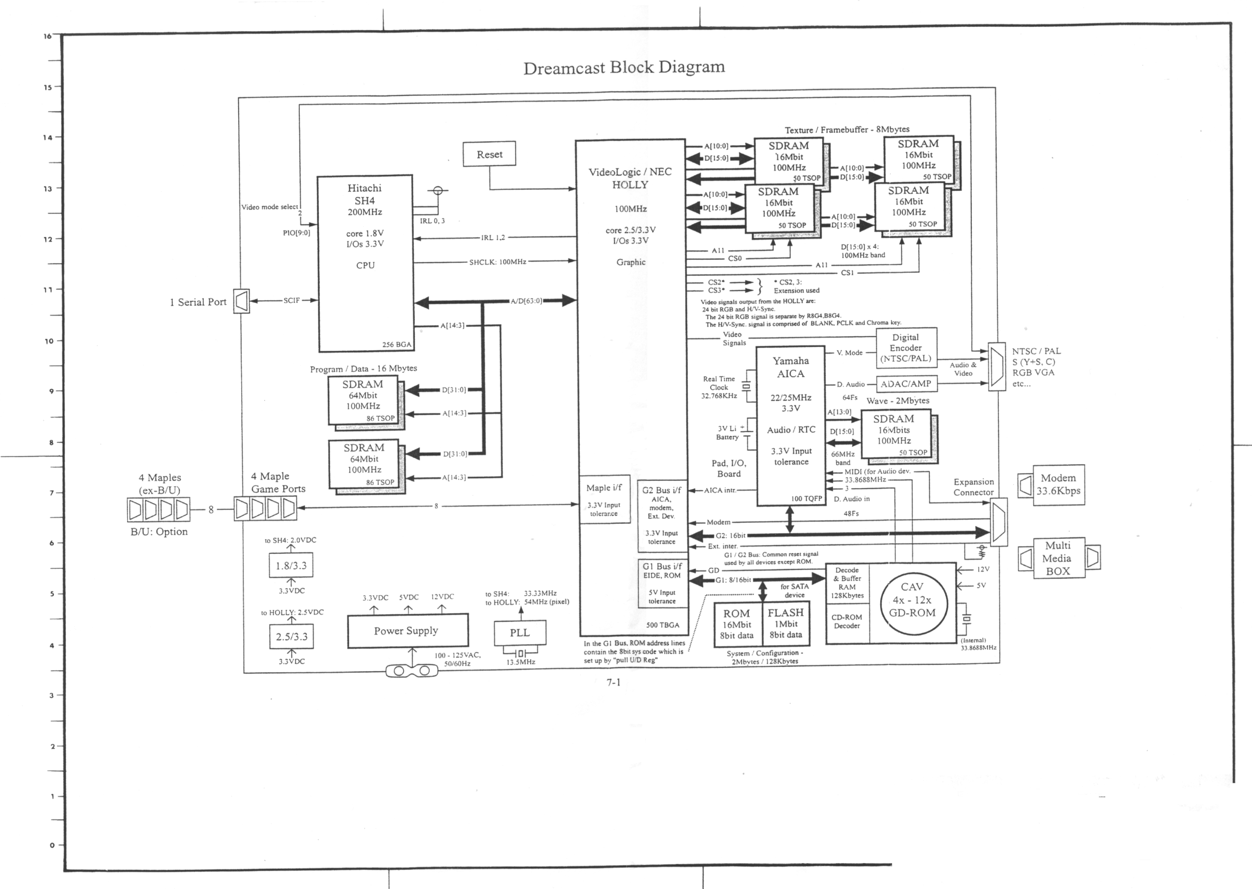
Sega's own block diagram for the Sega Dreamcast (VA0), sheet 7-1 of a Sega Dreamcast service manual. Extracted as an image from the PDF already hosted on this wiki at File:Sega Dreamcast VA0 Block Diagram.pdf so that it can be shown inline; the PDF remains the primary copy.
The sheet gives, in one page: the Hitachi SH4 at 200 MHz (1.8 V core, 3.3 V I/O, 256 BGA) and the VideoLogic / NEC HOLLY at 100 MHz (2.5/3.3 V core, 500 TBGA); every memory bank with its size and package; the G1, G2 and Maple buses with their voltage tolerances; the CAV 4x-12x GD-ROM drive with its 12 V and 5 V supplies and internal 33.8688 MHz clock; the modem and expansion connector; and the power supply, taking 100-125 VAC at 50/60 Hz and producing 3.3 V, 5 V and 12 V, with the two on-board regulator blocks that derive 2.0 V for the SH4 core and 2.5 V for the HOLLY core from the 3.3 V rail.
Source
[edit | edit source]

Sega Enterprises, Ltd., Dreamcast service documentation, sheet 7-1. Hosted on this wiki at File:Sega Dreamcast VA0 Block Diagram.pdf; see Sega Dreamcast VA0 Schematics.
Licensing
[edit | edit source]

Sega Enterprises, Ltd. factory service documentation, reproduced here for repair and preservation purposes. Sega has not released this material under a free licence and no claim of free licence is made. It is hosted because the hardware is long out of production and no supported service channel exists.
File history
Click on a date/time to view the file as it appeared at that time.
| Date/Time | Thumbnail | Dimensions | User | Comment | |
|---|---|---|---|---|---|
| current | 04:45, 23 September 2026 | | 3,722 × 2,642 (1.96 MB) | Josh (talk | contribs) | Sega Dreamcast block diagram sheet 7-1, extracted from the hosted PDF for inline display |
You cannot overwrite this file.
File usage
The following 2 pages use this file:
