

File:Sega Mega CD 2 main circuit board parts location.png

Summary
[edit | edit source]

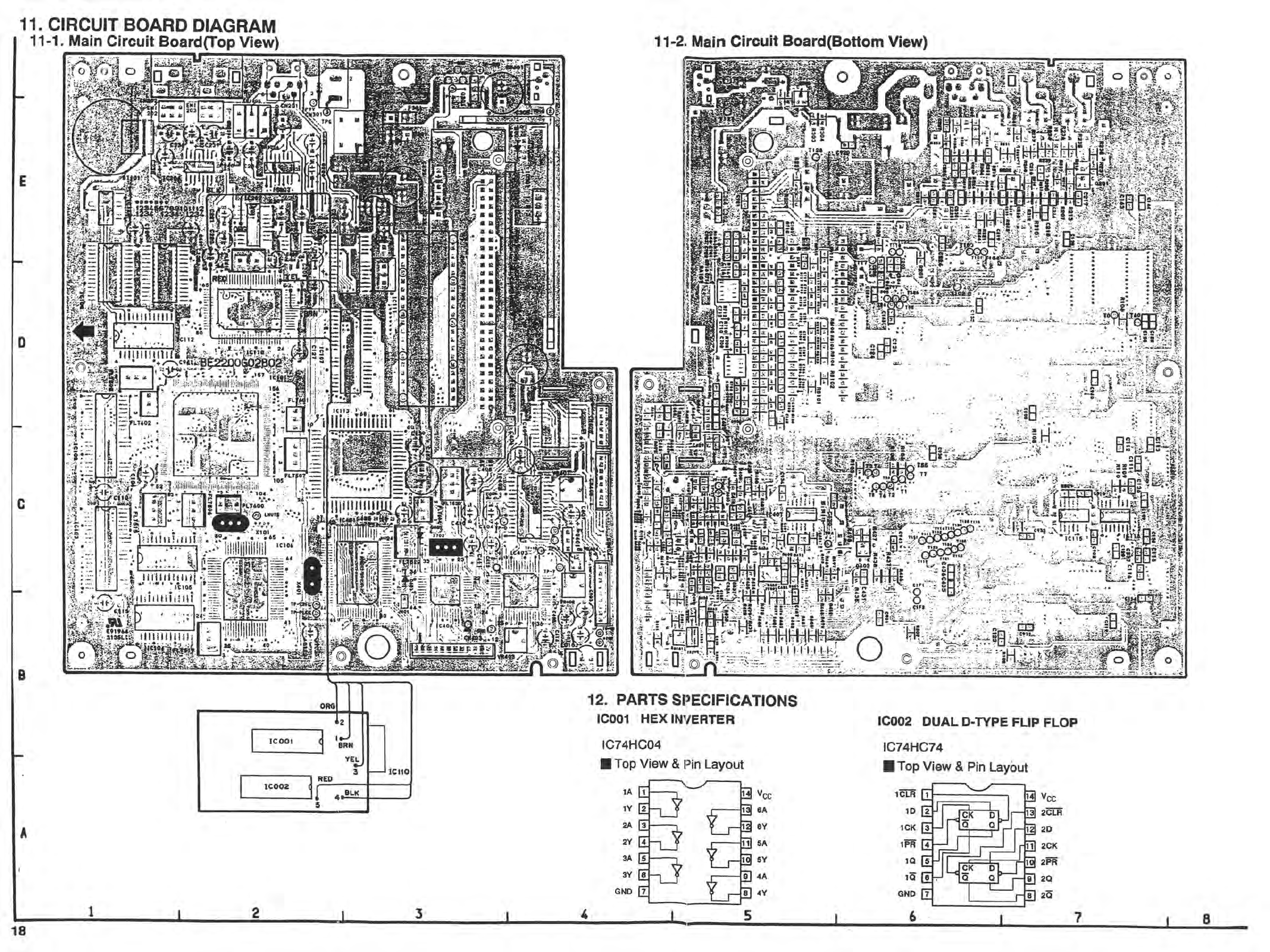
Sega's "11-1 / 11-2 Main Circuit Board (Top View and Bottom View)" diagrams for the main board of the Sega CD (Model 2), silkscreened BE2200G02, with the wiring of the small IC001/IC002 daughter board. Landmarks include the edge connector to the console, IC113 (68HC000), IC101 (MCE3), the CD front end (IC401 to IC404) with trimmers VR401 to VR403, IC301 (µPC2405 regulator) and F301.
Source
[edit | edit source]

Rendered from page 18 of the Service Manual, Sega CD II / Mega CD II, No. 002, August 1993 of File:Sega cd 2 - mega cd 2 - service manual.pdf, converted to greyscale PNG. Nothing else is altered.
Author
[edit | edit source]

Sega Enterprises, Ltd.
Licence
[edit | edit source]

Copyright Sega Enterprises, Ltd. Not freely licensed. A single page from a Sega service manual, hosted on the same basis as the complete manual.
File history
Click on a date/time to view the file as it appeared at that time.
| Date/Time | Thumbnail | Dimensions | User | Comment | |
|---|---|---|---|---|---|
| current | 21:25, 22 September 2026 | | 2,135 × 1,601 (3.45 MB) | Josh (talk | contribs) | Parts-location diagram from the Sega service manual already hosted here |
You cannot overwrite this file.
File usage
The following 3 pages use this file:
