

File:Sinclair ZX80 circuit diagram.png
Size of this preview: 460 × 599 pixels. Other resolution: 1,723 × 2,244 pixels.
Original file (1,723 × 2,244 pixels, file size: 445 KB, MIME type: image/png)
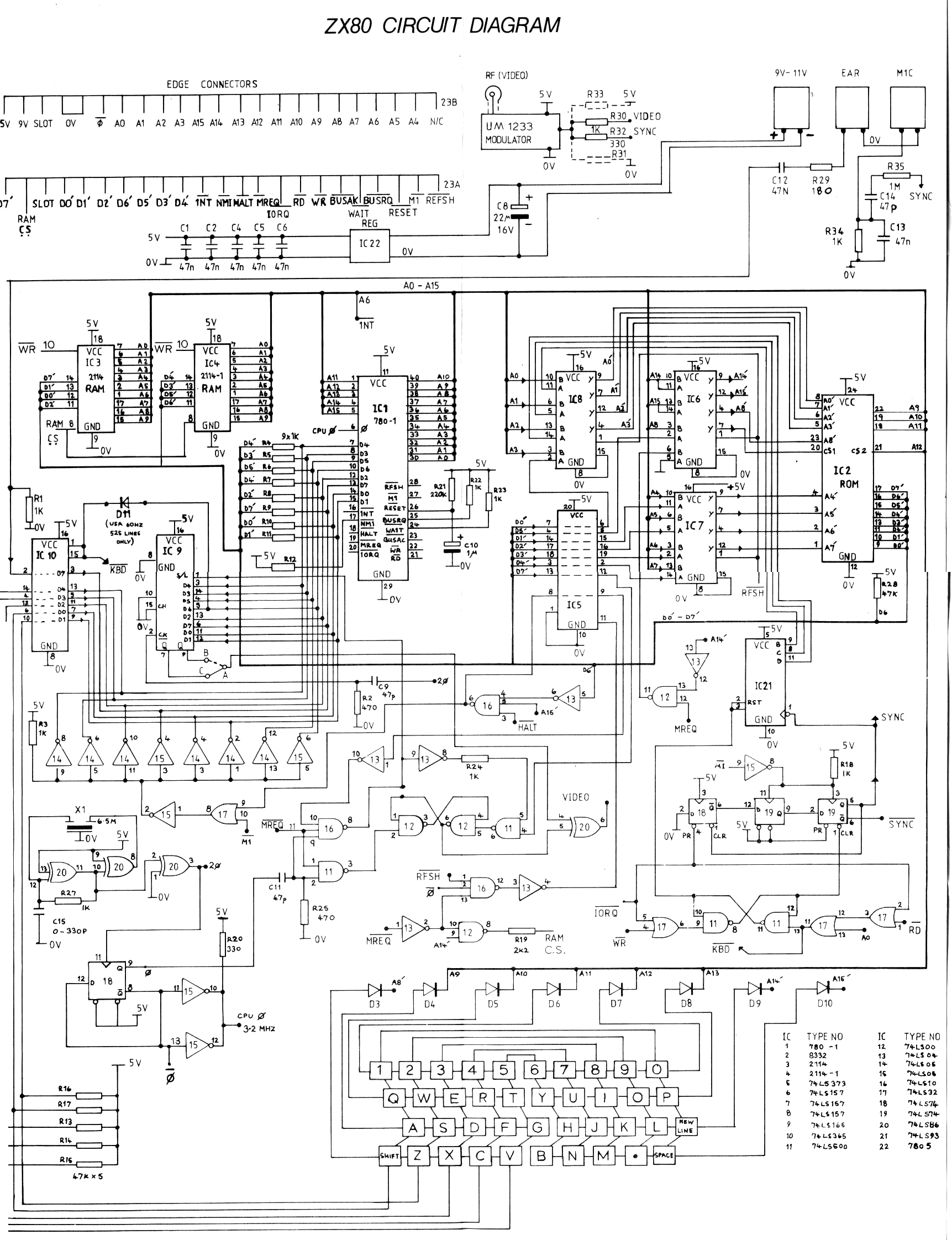
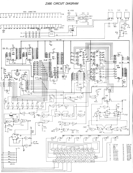
| Description | Sinclair ZX80 circuit diagram as published by Sinclair Research. Shows the 9 V - 11 V DC input with its 22 uF 16 V reservoir C8, the IC22 7805 regulator and the five 47 nF rail decouplers C1, C2, C4, C5 and C6, the R21/C10 power-on reset network on the Z80 (IC1), the 6.5 MHz crystal X1 and 3.25 MHz CPU clock, the 2114 static RAMs (IC3, IC4), the 8332 ROM (IC2), the all-discrete 74LS video and sync logic (the ZX80 has no ULA) and the UM1233 modulator. Also carries Sinclair's edge-connector pinout and the IC type list. |
|---|---|
| Source | Sinclair Research Ltd; scanned copy mirrored in the Sinclair ZX Computers Archive at k1.spdns.de. |
| Date | |
| Author | Sinclair Research Ltd |
| Licence | Used for archival / educational purposes with attribution. |
File history
Click on a date/time to view the file as it appeared at that time.
| Date/Time | Thumbnail | Dimensions | User | Comment | |
|---|---|---|---|---|---|
| current | 17:27, 22 September 2026 | | 1,723 × 2,244 (445 KB) | Josh (talk | contribs) | Sinclair ZX80 circuit diagram (Sinclair Research original) |
You cannot overwrite this file.
File usage
The following 2 pages use this file:
