
File:Amstrad PCW8256 monitor PCB layout.png
Size of this preview: 436 × 599 pixels. Other resolution: 1,602 × 2,200 pixels.

Original file (1,602 × 2,200 pixels, file size: 1.93 MB, MIME type: image/png)
Summary
edit
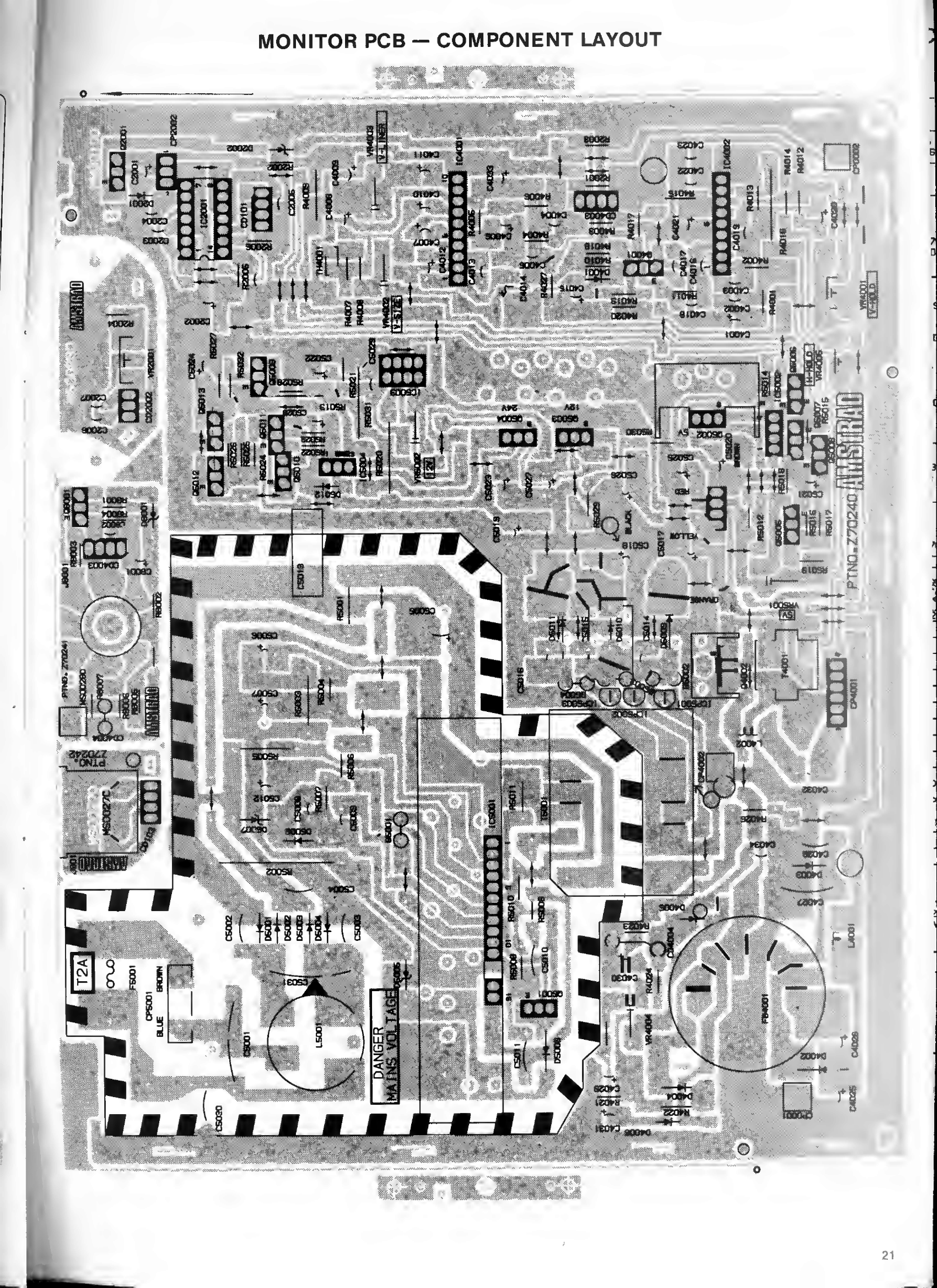
Component layout of the PCW8256/8512 monitor board, which carries the switch-mode power supply, the deflection circuits and the mains input with fuse F5001 (marked T2A). The hatched outline marks the area at mains potential ("danger mains voltage").
Source
edit
Rendered at 400 dpi from the hosted File:Amstrad PCW 8000 Series Service Manual.pdf (Amstrad, PCW 8256/8512 Personal Computer Word Processor Service Manual), PDF page 22, with the contrast increased.
Author
edit
Amstrad plc.
Licence
edit
Copyright Amstrad plc. Hosted for preservation and repair reference, with the source cited.
File history
Click on a date/time to view the file as it appeared at that time.
| Date/Time | Thumbnail | Dimensions | User | Comment | |
|---|---|---|---|---|---|
| current | 06:20, 2 October 2026 | | 1,602 × 2,200 (1.93 MB) | Josh (talk | contribs) | Upload for the Amstrad PCW/PPC pages |
You cannot overwrite this file.
File usage
The following 3 pages use this file:
