Sinclair ZX81
 | |
| Sinclair ZX81 – The Affordable Home Computer | |
| Specifications | |
|---|---|
| Manufacturer | Sinclair Research Ltd |
| Type | Home computer |
| Released | March 1981 |
| Discontinued | 1984 |
| Intro price | £69.95 kit / £89.95 ready-built (≈US$199/249 in 1981) |
| CPU | Zilog Z80A-compatible (NEC µPD780C) @ 3.25 MHz |
| Memory | 1 KB static RAM (expandable to 16 KB) |
| Storage | External cassette tape (300 baud, EAR/MIC jacks) |
| Display | Monochrome RF to TV – 32 × 24 text or 64 × 48 block-graphics |
| Sound | None (no audio hardware) |
| Dimensions | 200 mm × 150 mm × 35 mm (7.9 ″ × 5.9 ″ × 1.4 ″) |
| Weight | ≈ 400 g (0.88 lb) |
| OS / Firmware | 4 KB Sinclair BASIC in ROM |
| Predecessor | Sinclair ZX80 |
| Successor | Sinclair ZX Spectrum |
| Codename | “ZX81 project” |
| Model no. | ZX81 |
The Sinclair ZX81 is an 8-bit home computer launched by Sinclair Research in March 1981. It was designed as an affordable entry into computing, selling over 1.5 million units worldwide. The ZX81's compact design and low price made it accessible to a broad audience, contributing to the rise of home computing in the UK.
The ZX81 was notable for its simple design and was one of the first computers to be sold for under £100. It provided a platform for programming in BASIC and was widely used in schools and homes for educational purposes.
Architecture
[edit | edit source]- CPU – Z80A-class microprocessor clocked at 3.25 MHz.
- ROM – 8 KB mask ROM containing Sinclair BASIC and system routines.
- RAM – 1 KB of 2114 static RAM, expandable to 16 KB via the rear expansion bus.
- Logic – Utilizes standard TTL logic chips, with no custom chips.
Video generation
[edit | edit source]The ZX81 generates video output using the Z80 processor, which produces a sync pulse and fetches character data from RAM. The video output is interleaved with CPU operations, which can lead to display flicker during intensive processing.
Storage
[edit | edit source]The ZX81 uses the 300 baud Kansas City Standard for loading and saving programs via cassette tape. The average time to load a program is approximately 27 seconds per kilobyte.
I/O and Expansion
[edit | edit source]- Edge connector (40-way) – provides access to the Z80 bus, power, and video signals.
- 9 V DC input – unregulated power supply.
- RF modulator – outputs to channel 36 PAL TV.
Commercial accessories included:
- 1–16 KB RAM packs, ZX Printer, joystick interfaces, and various expansion modules.
Known PCB Revisions & Errata
[edit | edit source]| Issue | Visible Clues | Key Fixes / Changes |
|---|---|---|
| Issue 1 (Mar 1981) | “ZX81 Issue 1” silkscreen; no solder mask. | • Missing pull-up resistors on video output caused weak signals on some TVs.
• Early models had a tendency to overheat; later revisions included heatsinks. |
| Issue 2 (late 1982) | Added solder mask; improved layout. | • Enhanced power regulation for stability.
• Additional RAM compatibility improvements. |
General Maintenance
[edit | edit source]| Issue | Cause | Remedy |
|---|---|---|
| Flickering display | Poor power supply regulation | Replace with a regulated power supply. |
| Unresponsive keys | Wear on membrane keyboard | Replace keyboard or clean contacts. |
| Overheating | Lack of ventilation | Ensure proper airflow or add ventilation holes. |
Regular maintenance, including keyboard cleaning and power supply checks, is essential for longevity.
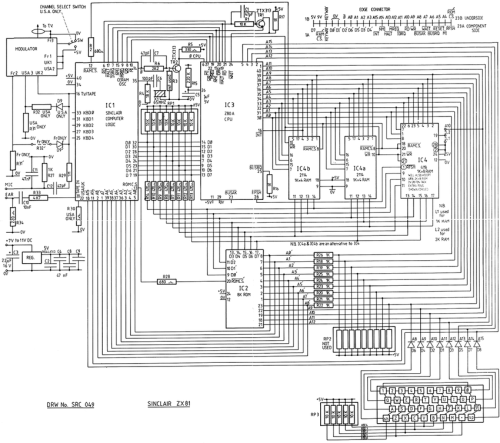
Schematic & PCB
[edit | edit source]The complete PCB schematic is available for reference.
 |
 |
|---|
Common Modifications
[edit | edit source]- 16 KB RAM upgrade – allows for more complex programs and reduces memory limitations.
- Composite video output mod – improves video quality for modern displays.
- Full-travel keyboard mod – replaces the membrane keyboard with a more tactile option.
ROM Keyword Map
[edit | edit source]Each key on the ZX81 keyboard has multiple functions depending on the mode selected:
| Key | F mode |
K mode |
L mode
|
|---|---|---|---|
| P | PRINT |
P |
(
|
| R | RETURN |
R |
)
|
| G | GOTO |
G |
>
|
Edge-Connector Pin-out
[edit | edit source]| Pin | Signal | Description | Pin | Signal | Description |
|---|---|---|---|---|---|
| 1 | A15 | Address bus MSB | 21 | D4 | Data bit 4 |
| 2 | A14 | 22 | D5 | ||
| 3 | A13 | 23 | D6 | ||
| 4 | A12 | 24 | D7 | ||
| 5 | A11 | 25 | BUSACK | Bus acknowledge | |
| 6 | A10 | 26 | BUSRQ | Bus request | |
| 7 | A9 | 27 | WAIT | Insert wait-states | |
| 8 | A8 | 28 | HALT |
