

Super Nintendo Entertainment System
 | |
 | |
| North American Super NES (SNS-001) with controller | |
| Specifications | |
|---|---|
| Manufacturer | Nintendo |
| Type | Home video game console |
| Released | Japan: 21 November 1990 North America: 23 August 1991 UK and Ireland: 11 April 1992[1] |
| Discontinued | Europe: 1998 North America: 1999 Japan: 25 September 2003[1] |
| Units sold | 49.10 million (Japan 17.17 million, the Americas 23.35 million, other regions 8.58 million)[2] |
| CPU | Ricoh 5A22 (65C816 core) at 3.58, 2.68 or 1.79 MHz, divided from a 21 MHz master clock[3] |
| Memory | 128 KB work RAM, 64 KB video RAM, 64 KB sound RAM[4] |
| Storage | Game Pak ROM cartridge, 62-pin connector |
| Display | — |
| Sound | Sony S-SMP and S-DSP, 8 channels, NEC µPD6376 DAC |
| Graphics | S-PPU1 and S-PPU2 picture processors |
| Power | North America: SNS-002, 10 V DC 850 mA Japan: 10 V DC PAL: NES-002 transformer, 9 V AC |
| OS / Firmware | None |
| Predecessor | Nintendo Entertainment System |
| Successor | Nintendo 64 |
| Model no. | SHVC-001 (Super Famicom), SNS-001 (North America), SNSP-001 (PAL), SNS-101 and SHVC-101 (New-Style SNES and Super Famicom Jr.)[5] |
The Super Nintendo Entertainment System (SNES) is Nintendo's 16-bit home video game console, sold in Japan as the Super Famicom. It was released in Japan on 21 November 1990, in North America on 23 August 1991 and in the UK and Ireland on 11 April 1992.[1] Nintendo's figures give 49.10 million consoles sold, 23.35 million of them in the Americas.[2]
Nintendo's Brazilian distributor Playtronic issued a Portuguese service manual for the console, the Manual Técnico do Super NES (Rev. 01/94), which is hosted here as Nintendo Super NES Technical Manual (Playtronic, Rev. 01-94). Nintendo's Japanese Famicom / Super Famicom / Game Boy service manual is hosted as Nintendo Famicom Service Manual. Most of the board-level figures below come from those two documents.[3]
For servicing see Super Nintendo General Maintenance, Super Nintendo Troubleshooting Guide and Super Nintendo Capacitor Replacement Guide. The Japanese console has its own set: Super Famicom Maintenance Guide, Super Famicom Troubleshooting Guide and Super Famicom Capacitor Replacement Guide.
Models
[edit | edit source]The original console was sold in three case styles. The Super Famicom (SHVC-001) and the PAL SNES (SNSP-001) share one rounded design; the North American and Brazilian SNS-001 has a squared-off case with purple switches. All NTSC consoles, Japanese, Korean and North American, use the same mainboard revisions.[5]
In 1997 Nintendo released the cost-reduced New-Style SNES (SNS-101) in North America, followed by the Super Famicom Jr. (SHVC-101) in Japan and a Brazilian version in 1998. It uses one board, SNN-CPU-01, has no eject button and no expansion port, and its Multi Out carries no S-Video or RGB. There was no PAL version.[5]
Architecture
[edit | edit source]The CPU is the Ricoh 5A22, a 65C816 core with the DMA controller and joypad interface on the same chip. A 21 MHz master clock goes to the CPU, both picture processors and the cartridge connector. The CPU divides it by 6, 8 or 12 to run at 3.58, 2.68 or 1.79 MHz, choosing the speed according to the device being addressed; DMA always runs at 2.68 MHz.[3]
The master clock frequency depends on the television standard: 21.47727 MHz on NTSC consoles, and 21.28137 MHz on PAL consoles, where the S-CLK chip synthesises it from a 17.734475 MHz crystal.[4] Brazilian consoles output PAL-M and use a 21.453666 MHz crystal.[3][5]
The reset section on the original board is a 4 MHz oscillator, a 74HCU04 hex inverter, the CIC lockout chip and the reset switch. The CIC releases PPU2 first, then PPU1, then the CPU, so that both picture processors are running before the CPU starts.[3] From the GPM boards onwards the CIC takes its clock from the sound circuit instead of a separate resonator.[5][4]
Memory and storage
[edit | edit source]The console has 128 KB of work RAM, 64 KB of video RAM and 64 KB of sound RAM, the last reachable only by the sound processor.[4] Programs come on Game Pak cartridges through a 62-pin connector. Some cartridges carry extra processors such as the Super FX, SA-1 or DSP-1, and battery-backed save RAM. The console itself has no battery. Nintendo's Game Pak test procedure expects a cartridge save battery to read between 2.7 and 3.2 V DC.[6]
Graphics and sound
[edit | edit source]Two picture processors, S-PPU1 (5C77) and S-PPU2 (5C78), work as a pair with two 32K × 8 video RAM chips. The standard picture is 256 × 224 pixels, with interlaced modes up to 512 × 448, and the palette holds 256 entries of 15-bit colour.[4]
The sound subsystem is the S-SMP sound processor (an SPC700 core), the S-DSP with eight sample channels, two 256 Kbit RAMs and a D/A converter. Its stereo output passes through an op-amp stage to the Multi Out; the RF modulator and the expansion port receive a mono mix.[3] On the SHVC-CPU-01 board most of the sound hardware is on a separate SHVC-SOUND daughterboard, which Nintendo sold as a service part. Later boards build it onto the mainboard, and the SNS-CPU-APU-01 and 1CHIP boards merge the S-SMP, S-DSP and sound RAM into one S-APU chip.[7][5]
Input, output and expansion
[edit | edit source]The two controller ports are on a small front board joined to the mainboard by an 11-way flat cable.[3] On PAL consoles that board puts diodes in the clock and strobe lines, so a controller without its own pull-up resistors may not work on a PAL console.[4]
The 12-pin Multi Out carries composite video, S-Video, RGB with sync, stereo audio and +5 V.[4] PAL boards add a voltage doubler that supplies about 12 V to the Multi Out for SCART switching; it works only when the console is fed AC.[5] The 28-pin expansion port on the underside was used by the Satellaview and the Exertainment bicycle.[4]
Earlier consoles have an anti-eject lever on the power switch that engages a notch in the cartridge. Cartridges with a diagonal notch push the lever and switch the console off as they are removed.[4] Nintendo dropped the lock bar on the GPM consoles and fitted a warning label instead.[3][5]
Power
[edit | edit source]| Item | Figure | Source and note |
|---|---|---|
| North American adapter | SNS-002, 10 V DC 850 mA, centre negative | Rating plate[8] |
| Japanese adapter | 10 V DC, same 5.5 × 2.1 mm plug as the Famicom | Nintendo's Super Famicom power diagram shows 13-14 V at the regulator input, and its Famicom HVC-002 adapter reads 13.5 ± 1.5 V with no load[7][5] |
| PAL adapter | Toy safety transformer such as the NES-002, 9 V AC | Nintendo's PAL booklet names the NES-002[9]; 9 V AC per fullsnes[4]. The board rectifies it |
| F1 | 1.5 A SSTR axial fuse | In both Nintendo parts lists[3][7] |
| Regulator | 7805 at U12; U9 on 1CHIP and SNN-CPU-01 boards | Nintendo shows 13-14 V in and 5 V out[7][10] |
| Vcc | 5 V regulated | Logic supply for the CPU, PPUs and sound chips[3][4] |
| Vs | About 7 V unregulated | Feeds the audio amplifier only. Without it the console runs but is silent[3][4] |
North American consoles use a power jack that a Famicom-style plug does not fit, which keeps an NES AC adapter out of a console that expects DC. The Super Famicom uses the same 5.5 × 2.1 mm jack as the Famicom.[5] From the SNS-CPU-GPM-02 onwards, North American boards replace the reverse-polarity diode with a 0 Ω link, so a centre-positive supply is not blocked.[5] PAL boards take AC through a bridge rectifier, or four discrete diodes on the 1CHIP boards.[5]
Board revisions
[edit | edit source]The revision is printed on the mainboard; the case and serial number do not identify it reliably.[5]
| Board | Region | Years | Main changes |
|---|---|---|---|
| SHVC-CPU-01 | NTSC (Japan, North America) | 1990-1992 | Original board, physically the largest. Sound on a plug-in SHVC-SOUND module; 4 MHz CIC resonator; C67 1000 µF reservoir, left off later US boards |
| SNS-CPU-GPM-01, -02 | NTSC | 1992-1994 | Ground Plane Method board: no lower RF shield, shorter PCB, sound built on, no 4 MHz oscillator. C67 is left off US boards. US GPM-02 boards drop the reverse-polarity diode |
| SNSM-CPU-GPM-02 | Brazil | 1993-1995 | PAL-M version of the GPM-02 |
| SNSP-CPU-01, -02 | PAL | 1992-1995 | AC input and bridge rectifier, S-CLK, SCART voltage doubler. Polarised C59 on the -01, bipolar on most -02 boards |
| SNS-CPU-RGB-01, -02 | NTSC | 1994-1995 | Cartridge connector soldered to the board; new RGB encoder; new audio DAC on the -02 |
| SNS-CPU-APU-01 | NTSC | 1995-1996 | S-SMP, S-DSP and sound RAM merged into the S-APU; last board with separate CPU and PPUs |
| SNS-CPU-1CHIP-01, -02, -03 | NTSC | 1995-1997 | CPU, PPU1 and PPU2 merged into the S-CPUN. The -03 omits the composite-sync parts |
| SNSP-CPU-1CHIP-01, -02 | PAL | 1995-1997 | PAL single-chip board; four diodes in place of the bridge rectifier |
| SNN-CPU-01 | SNS-101 and SHVC-101 | 1997 on | New-Style SNES and Super Famicom Jr. |
Sources: ConsoleMods for the list, years and changes;[5] Nintendo's Playtronic manual for the GPM changes;[3] Console5 for the chip and capacitor lists.[10]
"GPM" is a printed-circuit process; "1CHIP" is a later chip consolidation. A GPM board still has a separate CPU and two PPUs.[3][5]
Known faults
[edit | edit source]- SHVC-CPU-01 boards are prone to CPU and PPU failures and to leaking surface-mount capacitors.[5]
- 1CHIP and New-Style consoles can show a pale vertical line down the centre of the picture, traced to power filtering around the regulator.[11]
- SNSP-CPU-01 boards have a polarised capacitor at C59 that is prone to failure; Nintendo changed it to a bipolar part on most -02 boards.[5][10]
- Nintendo's own fault table puts the 62-pin cartridge connector first for a solid-colour screen, a scrambled picture and a frozen game.[3]
Diagnosis is covered in Super Nintendo Troubleshooting Guide.
Documentation
[edit | edit source]- Nintendo Super NES Technical Manual (Playtronic, Rev. 01-94): Nintendo's Portuguese service manual, with theory of operation, parts lists, disassembly, diagnostic tables and the GPM board.[3]
- Nintendo Famicom Service Manual: Nintendo's Japanese service manual for the Famicom, Super Famicom and Game Boy, issued 7 August 1992.[7]
- SNES Schematic: a community redraw of the NTSC GPM and RGB mainboards by Jonathon W. Donaldson, not a Nintendo document.
- Super Nintendo Entertainment System Bedienungsanleitung: Nintendo of Europe's German instruction booklet for the PAL console.[9]
Gallery
[edit | edit source]-
 North American SNS-001
 -
 Super Famicom (SHVC-001)
 -
 PAL SNES
 -
 North American controller
 -
 SNS-002 adapter and rating plate
 -
 SNS-CPU-RGB-01 board from a Super Famicom
 -
 SNS-CPU-APU-01 board, underside
 -
 SNSP-CPU-1CHIP-02 board
 -
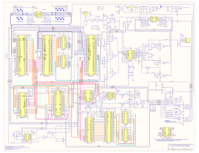 Community redraw of the NTSC schematic


Related pages
[edit | edit source]- Super Nintendo General Maintenance
- Super Nintendo Troubleshooting Guide
- Super Nintendo Capacitor Replacement Guide
- Super Famicom
- Nintendo Entertainment System
- Nintendo 64
- List of Nintendo Hardware
References
[edit | edit source]- ↑ 1.0 1.1 1.2 Wikipedia, "Super Nintendo Entertainment System", revision 1376345595 (retrieved 2026-10-01). Infobox release and discontinuation dates, with that article's own sources.
- ↑ 2.0 2.1 Nintendo Co., Ltd., Consolidated Sales Transition by Region (October 2015; retrieved 2026-10-01), "Super Family Computer/SNES" hardware, life-to-date figures in units of ten thousand.
- ↑ 3.00 3.01 3.02 3.03 3.04 3.05 3.06 3.07 3.08 3.09 3.10 3.11 3.12 3.13 3.14 Nintendo / Playtronic, Manual Técnico do Super NES, Rev. 01/94, hosted at Nintendo Super NES Technical Manual (Playtronic, Rev. 01-94). Pp. 2-1 and 2-2 (theory of operation: 10 V DC unregulated input, regulated Vcc 5 V and unregulated Vs 7 V for the audio amplifier, 21 MHz master clock divided by 6, 8 and 12, DMA at 2.68 MHz, controllers read about every 17 ms, reset section and the PPU2-PPU1-CPU reset order, eight-channel DSP and LM358 audio amplifier); pp. 2-6 to 2-8 (console parts list: RF5A22 CPU, RF5C77 PPU1, RF5C78 PPU2, 1 Mbit WRAM, two 256 Kbit SRAMs, F411 CIC, 1.5 A SSTR axial fuse, 7805, 4 MHz ceramic oscillator, 21.453666 MHz PAL-M crystal, upper and lower 62-pin connectors); p. 2-14 (disassembly, C67 discharge, six security screws); pp. 2-28 and 2-29 (console diagnostic table); p. 3-1 (GPM board).
- ↑ 4.00 4.01 4.02 4.03 4.04 4.05 4.06 4.07 4.08 4.09 4.10 4.11 Martin Korth, fullsnes (nocash SNES hardware specifications, retrieved 2026-10-01). Sections "SNES Memory" (128 KB WRAM, 64 KB VRAM, 64 KB sound RAM), "SNES Timing Oscillators" (NTSC 21.47727 MHz; PAL 17.734475 MHz crystal and 21.28137 MHz master clock from the S-CLK; 24.576 MHz APU oscillator; CIC clock 3.072 MHz), "SNES Audio/Video Connector Pinouts", "SNES Power Supply" (PAL 9 V AC, NTSC 10 V DC 850 mA through a diode; 7805; audio amplifier on the unregulated rail; anti-eject lever), "SNES Expansion Port (EXT) Pinouts" and "SNES Chipset" (SNSP-CPU-01 and single-chip board parts lists).
- ↑ 5.00 5.01 5.02 5.03 5.04 5.05 5.06 5.07 5.08 5.09 5.10 5.11 5.12 5.13 5.14 5.15 5.16 ConsoleMods Wiki, "SNES Model Differences" (revision 95480, retrieved 2026-10-01). Board revisions and their years, shared NTSC boards, PAL AC input and SCART voltage doubler, removal of the reverse-polarity diode on US boards from the GPM-02, CIC clock source on GPM boards, C67 omitted on later US consoles, 1CHIP and SNN-CPU-01 details. Secondary source.
- ↑ Nintendo / Playtronic, Manual Técnico do Super NES, Rev. 01/94, p. 7-6, Game Pak test procedure.
- ↑ 7.0 7.1 7.2 7.3 7.4 Nintendo, ファミコン・スーパーファミコン・ゲームボーイ サービスマニュアル (Famicom / Super Famicom / Game Boy Service Manual), hosted at Nintendo Famicom Service Manual. P. 6 (HVC-002 adapter: DC 13.5 ± 1.5 V with no load is normal); p. 11 (SHVC power-switch harness polarity, front unit and ferrite core); p. 12 (FFC orientation, SHVC power circuit with 13-14 V at the 7805 input); p. 15 (Super Famicom repair price list: sound module, 7805, crystal, 1.5 A SSTR fuse, 62-pin card connector upper and lower).
- ↑ Evan-Amos, "Nintendo-Super-NES-Power-Supply.jpg", Wikimedia Commons, public domain (retrieved 2026-10-01). Photograph of the SNS-002 rating plate: "Input AC120V 60Hz 17W, Output DC10V 850mA", "for use with Super NES and Virtual Boy only", with the centre-negative polarity symbol.
- ↑ 9.0 9.1 Nintendo of Europe, Super Nintendo Entertainment System Bedienungsanleitung, PAL version, form HW(G)-SNSP-NOE, p. 9, hosted as File:Super Nintendo Entertainment System Bedienungsanleitung HW(G)-SNSP-NOE.pdf. The console may only be run from a toy safety transformer such as the Nintendo NES-002, to VDE 0551.
- ↑ 10.0 10.1 10.2 Console5 TechWiki, "SNES" (retrieved 2026-10-01). Chip lists by board revision, capacitor lists, and a transcription of Nintendo's control-deck diagnostic table. Secondary source.
- ↑ Bob, "Restoring A Super Nintendo", RetroRGB, 31 May 2020 (retrieved 2026-10-01). The SNES is not known for leaking capacitors but they should be checked; damage hides under surface-mount capacitors; cartridge-connector cleaning; the white-line fix (78S05 regulator, larger output capacitor) on 1CHIP and New-Style consoles; the 1CHIP ghosting fix at C11.
