

Macintosh SE/30 Reloaded Logic Board: Difference between revisions
Rebuilt from the project repository README: DELETED unsourced infobox (4-layer PCB, 2023, model SE30RL), the F1/F3/D3 fuse-and-diode troubleshooting rows, the UE8 claim and the no-electrolytics/32-bit-clean-ROM feature claims; added the six reverse-engineered PALs with their board locations and Apple part numbers, the CC-BY-NC-SA licence, the ATF16V8B/C device caution, and consistency checks against Apples own SE/30 documentation; stray </div> tags and malformed table attributes fixed; refs a... |
|||
| (5 intermediate revisions by the same user not shown) | |||
| Line 1: | Line 1: | ||
[[File:SE30_Reloaded_Board.jpg|thumb|250px|Assembled SE/30 Reloaded logic board]] | |||
The '''Macintosh SE/30 Reloaded logic board''' is a modern recreation of the [[Macintosh SE/30]] main logic board, published by Bolle. It is '''not a 1:1 copy''': the original schematics were used to redesign and re-route a lookalike board.<ref name="repo">TheRealBolle, ''Macintosh SE/30 logicboard recreation'', project repository README — design basis, reverse-engineered PALs and their board locations, licence and board-file notes. https://github.com/TheRealBolle/SE30</ref> | |||
The project files are released under '''CC-BY-NC-SA''' and are explicitly not intended for commercial use.<ref name="repo" /> | |||
This page covers the recreation board. For the original machine see [[Macintosh SE/30]]; for repairing an original board, [[Macintosh SE/30 General Maintenance]] and the [[Macintosh SE/30 Capacitor Replacement Guide]]. | |||
== Why the board exists == | |||
An original SE/30 logic board fails in one characteristic way: its surface-mount electrolytic capacitors leak, the electrolyte corrodes traces and vias, and by the time the symptoms are obvious the damage is under the components. Boards that have lost traces in the video or sound sections are repairable but tedious, and some are beyond it. A new board lets the Apple-specific silicon from a damaged board be reused. | |||
== What the project reproduces, and what it does not == | |||
'''Reproduced.''' The board itself, and the programmable logic. The original PALs were reverse-engineered and their equations rewritten to match the behaviour of the originals; the JEDEC files supplied are '''not''' dumps of the original devices. They target 16V8-type parts — GAL16V8, PALCE16V8 or ATF16V8.<ref name="repo" /> | |||
The '''Macintosh SE/30 | |||
<templatestyles src="Template:StyledTable/styles.css" /> | <templatestyles src="Template:StyledTable/styles.css" /> | ||
{| class="wikitable styled-table" | {| class="wikitable styled-table" style="width:60%;" | ||
! | |+ '''Reverse-engineered PALs and their original Apple part numbers'''<ref name="repo" /> | ||
! Board location !! Original Apple part | |||
|- | |||
| UI6 || 341-0665-A | |||
|- | |- | ||
| | | UH7 || 341S0689-C | ||
|- | |- | ||
| | | UG6 || 341-0747-A | ||
|- | |- | ||
| | | UG7 || 341-0746-A | ||
|- | |- | ||
| | | UE6 || 341-0754-A | ||
|- | |||
| UE7 || 341-0755-A | |||
|} | |} | ||
== | '''Device caution from the project:''' certain low-power '''ATF16V8B''' parts do not work, and '''ATF16V8C''' parts use pin keepers rather than internal pull-ups and may also be problematic.<ref name="repo" /> | ||
''' | |||
{| class="wikitable" | '''Not reproduced.''' Apple's custom devices — the CPU support ASICs, the sound and floppy controllers, the ROM — are not part of the project. They have to come from a donor logic board or from the parts market, which is why a corroded original is worth keeping rather than scrapping. | ||
! | |||
== Files and manufacture == | |||
The gerbers are generated with the JLCPCB EAGLE CAM job files and the pick-and-place data is intended for JLCPCB; other manufacturers may require different output. A bill of materials is published with the project.<ref name="repo" /> | |||
== Consistency with the original == | |||
Two things are worth checking against the original machine's documentation rather than assumed: | |||
* The SE/30's screen does '''not''' come out of main memory. The logic board carries a separate 64 KB video display RAM and an 8192-byte video declaration ROM mapped at $FE00 0000, which Apple calls pseudo-slot video. Any recreation has to provide both.<ref name="gtmfh">Apple Computer, ''Guide to the Macintosh Family Hardware'', 2nd edition, Addison-Wesley, 1990, Chapter 12 "Displays", pp. 408–409.</ref> | |||
* The memory rules are the original machine's rules: eight 30-pin SIMM sockets in two banks of four, 120 ns or faster, eight chips per module, banks filled completely, larger modules in bank A.<ref name="gtmfh2">Apple Computer, ''Guide to the Macintosh Family Hardware'', 2nd edition, Addison-Wesley, 1990, Chapter 5 "Memory", pp. 208–211.</ref> See [[Macintosh SE/30 Memory Upgrade Guide]]. | |||
For tracing signals during a build, the MIT-licensed KiCad recreation of Apple engineering drawing '''050-0253-01''' hosted here is the most usable reference, and its pin matrices give the device at each location — UK8 CPU, UI5 FPU, UI8 GLUE, UK12/UK11 VIA1/VIA2, UJ11 SWIM, UI12 SCSI, UG12 SCC, UK6 video ROM, UC6/UC7 VRAM, J13 PDS.<ref name="redraw">''Macintosh SE/30 Logic Board Schematic Redraw'', KiCad recreation of Apple engineering drawing 050-0253-01, MIT licence. Hosted on this wiki: [[:File:Macintosh SE30 Logic Board Schematic Redraw 050-0253-01.pdf]].</ref> | |||
== Assembly == | |||
=== Before you start === | |||
{| class="wikitable styled-table" style="width:75%;" | |||
! Step !! Detail | |||
|- | |||
| '''Clean''' || Isopropyl alcohol (>90 %) and a lint-free wipe, both sides. | |||
|- | |||
| '''Inspect''' || Under magnification, look for shorts, lifted pads and fabrication defects before any part is fitted. | |||
|- | |||
| '''Dry fit''' || Offer up sockets and the large connectors to check alignment. | |||
|- | |- | ||
| | | '''ESD''' || Grounded wriststrap and an ESD-safe surface throughout. | ||
| | |||
|} | |} | ||
=== | === Soldering === | ||
{| class="wikitable styled-table" style="width:75%;" | |||
{| class="wikitable" | |||
! Component !! Technique | ! Component !! Technique | ||
|- | |- | ||
| 0402/0603 passives || | | 0402/0603 passives || Tin one pad, place the part, solder the second pad, then reflow the first. | ||
|- | |||
| SOIC and QFP || Drag soldering or pin-by-pin, with plenty of flux. | |||
|- | |- | ||
| | | PLCC || Tack opposite corners first, check seating, then solder the remaining leads. | ||
|- | |- | ||
| | | Through-hole || Tack one pin, confirm the part is square and flush, then solder the rest and trim. | ||
|} | |} | ||
Use sockets for the CPU, FPU and ROM unless you are certain you will never need to swap them. | |||
[[File:Through_Hole_Connectors.jpg|thumb|center|Through-hole connector installation]] | |||
== | === Suggested order === | ||
# Power-related | # Power-related parts and the oscillator | ||
# | # Surface-mount passives | ||
# | # Surface-mount ICs and transistors | ||
# PLCC | # PLCC and DIP sockets, SIMM sockets | ||
# | # Connectors, headers, switches and jacks | ||
== | == First power-up == | ||
== | |||
* Bring it up on a current-limited bench supply, not in the machine. | |||
* Check the resistance between +5 V and ground before applying power; a dead short means a bridge or a reversed part. | |||
{| class="wikitable" | * Verify each rail, then check for parts running hot. | ||
* Only once the board is stable on the bench should it go into a chassis — where the CRT makes probing hazardous. Read [[CRT Discharge Procedure]] first. | |||
{| class="wikitable styled-table" style="width:70%;" | |||
! Subsystem !! Test | ! Subsystem !! Test | ||
|- | |- | ||
| ROM | | ROM and CPU || Boot chime and something on screen | ||
|- | |- | ||
| RAM || | | RAM || Boots, and the reported total matches what is fitted | ||
|- | |- | ||
| Video || | | Video || Stable raster, correct geometry | ||
|- | |- | ||
| Sound || | | Sound || Startup chime, then software playback | ||
|- | |- | ||
| ADB || | | ADB || Keyboard and mouse respond | ||
|- | |- | ||
| SCSI | | SCSI and floppy || Boot from known-good media; check termination | ||
|} | |} | ||
== Troubleshooting == | == Troubleshooting a build == | ||
[[File:Simasimac issue.jpg|center|thumb|Simasimac | |||
{| class="wikitable" | [[File:Simasimac issue.jpg|center|thumb|Simasimac]] | ||
! Symptom !! | |||
{| class="wikitable styled-table" style="width:75%;" | |||
! Symptom !! Where to look | |||
|- | |- | ||
| | | No boot, black screen || Oscillator, reset line, CPU orientation and socket seating | ||
|- | |- | ||
| | | Simasimac (striped raster) || ROM access — socket seating, ROM SIMM contacts, and the RAM-signalling PALs | ||
|- | |- | ||
| | | Death chimes || RAM: seating, bank population, SIMM speed, and the RAM-signalling PALs | ||
|- | |- | ||
| No | | No video, machine otherwise alive || Video ROM and the video PALs at UE6/UE7/UG6/UG7 | ||
|- | |- | ||
| No floppy | | No ADB, no floppy, no SCSI || Solder joints on the relevant connector and its support parts; then the donor ASIC | ||
|} | |} | ||
Faults specific to a hand-built board are overwhelmingly solder faults and wrong or missing programmable parts, not design faults. Compare a suspect signal against the schematic redraw before replacing anything. | |||
== Community | == Community resources == | ||
* [https:// | |||
* [https:// | * [https://github.com/TheRealBolle/SE30 Project repository — schematics, gerbers, JEDEC files and BOM] | ||
* [https:// | * [https://68kmla.org 68kMLA forum] — build threads and troubleshooting | ||
* [https://tinkerdifferent.com TinkerDifferent] | |||
== Gallery == | == Gallery == | ||
<gallery> | <gallery> | ||
File:SE30 Reloaded.jpg|Assembled board | |||
File:SMD Soldering Technique.jpg|SMD soldering | File:SMD Soldering Technique.jpg|SMD soldering | ||
File:Simasimac issue.jpg|Simasimac | File:Simasimac issue.jpg|Simasimac | ||
File:Through Hole Connectors.jpg|Through | File:Through Hole Connectors.jpg|Through-hole soldering | ||
</gallery> | </gallery> | ||
== Related pages == | |||
* [[Macintosh SE/30]] | |||
* [[Macintosh SE/30 General Maintenance]] | |||
* [[Macintosh SE/30 Capacitor Replacement Guide]] | |||
* [[Macintosh SE/30 Memory Upgrade Guide]] | |||
* [[Recommended Tools]] | |||
== References == | |||
<references /> | |||
[[Category:Apple Vintage Computers]] | [[Category:Apple Vintage Computers]] | ||
Latest revision as of 18:21, 23 September 2026

The Macintosh SE/30 Reloaded logic board is a modern recreation of the Macintosh SE/30 main logic board, published by Bolle. It is not a 1:1 copy: the original schematics were used to redesign and re-route a lookalike board.[1]
The project files are released under CC-BY-NC-SA and are explicitly not intended for commercial use.[1]
This page covers the recreation board. For the original machine see Macintosh SE/30; for repairing an original board, Macintosh SE/30 General Maintenance and the Macintosh SE/30 Capacitor Replacement Guide.
Why the board exists
[edit | edit source]An original SE/30 logic board fails in one characteristic way: its surface-mount electrolytic capacitors leak, the electrolyte corrodes traces and vias, and by the time the symptoms are obvious the damage is under the components. Boards that have lost traces in the video or sound sections are repairable but tedious, and some are beyond it. A new board lets the Apple-specific silicon from a damaged board be reused.
What the project reproduces, and what it does not
[edit | edit source]Reproduced. The board itself, and the programmable logic. The original PALs were reverse-engineered and their equations rewritten to match the behaviour of the originals; the JEDEC files supplied are not dumps of the original devices. They target 16V8-type parts — GAL16V8, PALCE16V8 or ATF16V8.[1]
| Board location | Original Apple part |
|---|---|
| UI6 | 341-0665-A |
| UH7 | 341S0689-C |
| UG6 | 341-0747-A |
| UG7 | 341-0746-A |
| UE6 | 341-0754-A |
| UE7 | 341-0755-A |
Device caution from the project: certain low-power ATF16V8B parts do not work, and ATF16V8C parts use pin keepers rather than internal pull-ups and may also be problematic.[1]
Not reproduced. Apple's custom devices — the CPU support ASICs, the sound and floppy controllers, the ROM — are not part of the project. They have to come from a donor logic board or from the parts market, which is why a corroded original is worth keeping rather than scrapping.
Files and manufacture
[edit | edit source]The gerbers are generated with the JLCPCB EAGLE CAM job files and the pick-and-place data is intended for JLCPCB; other manufacturers may require different output. A bill of materials is published with the project.[1]
Consistency with the original
[edit | edit source]Two things are worth checking against the original machine's documentation rather than assumed:
- The SE/30's screen does not come out of main memory. The logic board carries a separate 64 KB video display RAM and an 8192-byte video declaration ROM mapped at $FE00 0000, which Apple calls pseudo-slot video. Any recreation has to provide both.[2]
- The memory rules are the original machine's rules: eight 30-pin SIMM sockets in two banks of four, 120 ns or faster, eight chips per module, banks filled completely, larger modules in bank A.[3] See Macintosh SE/30 Memory Upgrade Guide.
For tracing signals during a build, the MIT-licensed KiCad recreation of Apple engineering drawing 050-0253-01 hosted here is the most usable reference, and its pin matrices give the device at each location — UK8 CPU, UI5 FPU, UI8 GLUE, UK12/UK11 VIA1/VIA2, UJ11 SWIM, UI12 SCSI, UG12 SCC, UK6 video ROM, UC6/UC7 VRAM, J13 PDS.[4]
Assembly
[edit | edit source]Before you start
[edit | edit source]| Step | Detail |
|---|---|
| Clean | Isopropyl alcohol (>90 %) and a lint-free wipe, both sides. |
| Inspect | Under magnification, look for shorts, lifted pads and fabrication defects before any part is fitted. |
| Dry fit | Offer up sockets and the large connectors to check alignment. |
| ESD | Grounded wriststrap and an ESD-safe surface throughout. |
Soldering
[edit | edit source]| Component | Technique |
|---|---|
| 0402/0603 passives | Tin one pad, place the part, solder the second pad, then reflow the first. |
| SOIC and QFP | Drag soldering or pin-by-pin, with plenty of flux. |
| PLCC | Tack opposite corners first, check seating, then solder the remaining leads. |
| Through-hole | Tack one pin, confirm the part is square and flush, then solder the rest and trim. |
Use sockets for the CPU, FPU and ROM unless you are certain you will never need to swap them.

Suggested order
[edit | edit source]- Power-related parts and the oscillator
- Surface-mount passives
- Surface-mount ICs and transistors
- PLCC and DIP sockets, SIMM sockets
- Connectors, headers, switches and jacks
First power-up
[edit | edit source]- Bring it up on a current-limited bench supply, not in the machine.
- Check the resistance between +5 V and ground before applying power; a dead short means a bridge or a reversed part.
- Verify each rail, then check for parts running hot.
- Only once the board is stable on the bench should it go into a chassis — where the CRT makes probing hazardous. Read CRT Discharge Procedure first.
| Subsystem | Test |
|---|---|
| ROM and CPU | Boot chime and something on screen |
| RAM | Boots, and the reported total matches what is fitted |
| Video | Stable raster, correct geometry |
| Sound | Startup chime, then software playback |
| ADB | Keyboard and mouse respond |
| SCSI and floppy | Boot from known-good media; check termination |
Troubleshooting a build
[edit | edit source]
| Symptom | Where to look |
|---|---|
| No boot, black screen | Oscillator, reset line, CPU orientation and socket seating |
| Simasimac (striped raster) | ROM access — socket seating, ROM SIMM contacts, and the RAM-signalling PALs |
| Death chimes | RAM: seating, bank population, SIMM speed, and the RAM-signalling PALs |
| No video, machine otherwise alive | Video ROM and the video PALs at UE6/UE7/UG6/UG7 |
| No ADB, no floppy, no SCSI | Solder joints on the relevant connector and its support parts; then the donor ASIC |
Faults specific to a hand-built board are overwhelmingly solder faults and wrong or missing programmable parts, not design faults. Compare a suspect signal against the schematic redraw before replacing anything.
Community resources
[edit | edit source]- Project repository — schematics, gerbers, JEDEC files and BOM
- 68kMLA forum — build threads and troubleshooting
- TinkerDifferent
Gallery
[edit | edit source]-
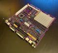 Assembled board
 -
 SMD soldering
 -
 Simasimac
 -
 Through-hole soldering


Related pages
[edit | edit source]- Macintosh SE/30
- Macintosh SE/30 General Maintenance
- Macintosh SE/30 Capacitor Replacement Guide
- Macintosh SE/30 Memory Upgrade Guide
- Recommended Tools
References
[edit | edit source]- ↑ 1.0 1.1 1.2 1.3 1.4 1.5 TheRealBolle, Macintosh SE/30 logicboard recreation, project repository README — design basis, reverse-engineered PALs and their board locations, licence and board-file notes. https://github.com/TheRealBolle/SE30
- ↑ Apple Computer, Guide to the Macintosh Family Hardware, 2nd edition, Addison-Wesley, 1990, Chapter 12 "Displays", pp. 408–409.
- ↑ Apple Computer, Guide to the Macintosh Family Hardware, 2nd edition, Addison-Wesley, 1990, Chapter 5 "Memory", pp. 208–211.
- ↑ Macintosh SE/30 Logic Board Schematic Redraw, KiCad recreation of Apple engineering drawing 050-0253-01, MIT licence. Hosted on this wiki: File:Macintosh SE30 Logic Board Schematic Redraw 050-0253-01.pdf.